
Choosing an Fpga Integrated Circuit is rarely a simple comparison of speed, price, and package size. The right device must fit the entire design, from sensor inputs to firmware updates. A small evaluation board can reveal problems that datasheets hide. Watch the clock signals. Measure heat near the voltage regulators. Check whether the available logic blocks match your planned architecture.
Steve Trimberger, an FPGA pioneer and former Xilinx chief scientist, described the technology’s central value clearly: “An FPGA is a programmable hardware device.” That flexibility matters, but it can also encourage careless decisions. More logic is not always better. Extra resources may increase power consumption, configuration time, and development effort. Your team should examine logic cells, DSP slices, embedded memory, I/O standards, transceivers, security features, and long-term availability.
Look beyond the headline specifications. Ask how easily the chip integrates with your tools, operating system, and verification flow. Confirm thermal limits under real workloads, not only laboratory demonstrations. Review vendor support, documentation quality, reference designs, and production history. A cheaper device may create expensive redesign work later.
No checklist is perfect. I have seen promising designs fail because engineers ignored package constraints or underestimated timing closure. That lesson deserves attention. Choosing well means balancing performance, reliability, cost, supply continuity, and engineering confidence. The best Fpga Integrated Circuit is not the most powerful option. It is the one your team can validate, manufacture, maintain, and improve without unpleasant surprises.
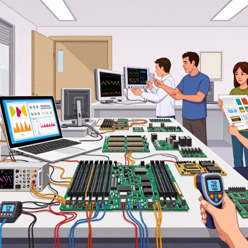
Before choosing an FPGA integrated circuit, define what the system must actually do. Record input and output standards, processing speed, memory needs, power limits, operating temperature, and physical size. A camera controller may need several high-speed interfaces, while a battery sensor node may value low leakage more than logic capacity. Write measurable targets, not vague goals. “Fast” is not a specification.
Tip 1: Build a requirement table. Include normal, minimum, and worst-case conditions.
Tip 2: Separate essential features from convenient features. This prevents unused resources from increasing cost and power.
Check timing margins, clock stability, pin availability, and configuration requirements before comparing devices. Estimate logic, memory, and arithmetic resources with at least 20 percent spare capacity. My early estimates were too optimistic because I ignored debugging signals and future firmware changes. That mistake forced a board revision. Review the design with hardware, software, and manufacturing engineers. Their concerns often expose hidden constraints. Also examine thermal behavior inside the real enclosure, not only on an open laboratory bench. Confirm every critical value against official electrical specifications and independent test results. Keep a written assumptions log. It will reveal where the design is still uncertain.

Choosing an FPGA starts with the architecture, not the package label. Examine the balance between lookup tables, registers, memory blocks, and routing resources. A device with abundant logic may still struggle if interconnect paths create timing delays. Check whether the architecture supports your data flow, clock domains, and expected parallel operations. Practical evaluation matters.
Estimate logic capacity from real design data, not optimistic guesses. Include control logic, interfaces, error handling, and future revisions. Leave useful headroom, often 20 to 30 percent, for routing and unexpected growth. I once underestimated buffering needs in a sensor project. The design fit, but timing closure became painful. That mistake changed my selection process.
Processing resources deserve equal attention. Dedicated multipliers, digital signal blocks, embedded processors, and high-speed memory can reduce logic usage significantly. Compare their quantity, operating range, and connection to internal memory. A processor may simplify control tasks, while parallel hardware handles repetitive calculations faster. Test a small representative module before committing to a large device. Simulations can mislead when physical routing is ignored. Build a trial layout with realistic clocks and input widths. Measure utilization, latency, power, and temperature under continuous load. Datasheet values provide authority, but board-level measurements provide confidence. Be willing to revise the choice. The cheapest fit is not always the most reliable fit.
10 Tips for Choosing an FPGA Integrated Circuit
Tip 1: Compare power consumption under realistic workloads, not only the quoted idle figure. A design running several clock domains can draw far more power than expected. Check static and dynamic power separately. Then estimate voltage losses across regulators. I once trusted a typical-value table and underestimated heat by nearly 20 percent. That mistake forced a board redesign.
Tip 2: Match performance with the actual workload. Higher logic capacity does not always mean faster operation. Review maximum clock frequency, memory bandwidth, latency, and available processing resources. Test a small prototype when possible. Short benchmarks reveal bottlenecks. A spreadsheet can still mislead.
Tip 3: Treat thermal requirements as a design limit. Calculate junction temperature using ambient temperature, package resistance, airflow, and heat-sink performance. Measure the board near the hottest operating condition. A thermal camera helps locate unexpected hot spots, but it cannot replace reliable sensor data. Leave practical margin for blocked vents, dust, and aging fans. Quiet cooling is not always sufficient.
Tip 4: Recheck power and performance together. Raising the clock may improve throughput but increase heat sharply. Lowering voltage can save energy, yet timing margins may shrink. Document these trade-offs in a verification report. Independent engineering review improves reliability, especially when field conditions differ from laboratory tests. Deliberate conservatism usually costs less than emergency thermal fixes.
| Tip | Selection Dimension | What to Compare | Typical Engineering Data | Recommended Decision Rule |
|---|---|---|---|---|
| 1 | Logic Capacity | Look-up tables, configurable logic blocks, flip-flops, and available logic utilization. | Small devices: approximately 1,000–20,000 logic elements. Mid-range devices: approximately 20,000–200,000 logic elements. High-capacity devices: above 200,000 logic elements. | Choose a device that uses no more than about 70–80% of its logic resources after routing, leaving room for design growth and timing optimization. |
| 2 | Power Consumption | Separate static power from dynamic power and evaluate voltage, clock frequency, switching activity, and utilization. | Static power: commonly from tens of milliwatts to several watts, depending on process technology and device size. Dynamic power: strongly dependent on clock rate, capacitance, voltage, and signal activity. | Use a power-estimation tool with realistic toggle rates and operating conditions rather than relying only on the maximum power value in a data sheet. |
| 3 | Core and I/O Voltage | Compare internal core voltage, auxiliary voltage, and supported I/O standards. | Many modern FPGA cores operate around 0.8–1.2 V. Common I/O supply ranges include approximately 1.2–3.3 V, depending on the I/O bank and standard. | Verify that the FPGA voltage rails match the available power tree and that level-shifting requirements do not add unacceptable cost, power, or board complexity. |
| 4 | Performance and Clock Speed | Evaluate maximum achievable clock frequency, timing margin, DSP performance, and worst-case process, voltage, and temperature conditions. | Typical user designs may operate from tens of megahertz to several hundred megahertz. Advanced digital signal-processing paths can reach higher rates when properly pipelined. | Compare application-level throughput and timing closure results, not only the advertised maximum clock frequency. |
| 5 | Embedded Memory | Check block RAM capacity, memory width, port configuration, distributed memory, and error-correction options. | Embedded memory may range from approximately tens of kilobits in small devices to tens of megabits in larger devices. Typical block sizes include 18–36 Kb, although implementations vary. | Select enough memory for buffering, packet storage, coefficient tables, and state machines without forcing excessive use of general logic resources. |
| 6 | DSP and Arithmetic Resources | Compare the number of dedicated multipliers, accumulators, pre-adders, and supported operand widths. | Dedicated DSP blocks commonly support operations such as 18 × 18-bit or 27 × 27-bit multiplication, with larger devices providing hundreds or more blocks. | For filtering, motor control, software-defined radio, or imaging, prioritize dedicated DSP blocks over implementing multipliers entirely with general logic. |
| 7 | I/O Count and Interfaces | Check user I/O quantity, differential-pair availability, I/O bank grouping, impedance control, and supported interfaces. | Available user I/O may range from approximately 20 to more than 1,000 pins, depending on package and device size. Differential interfaces commonly support standards such as LVDS. | Count signal pins, power pins, configuration pins, and reserved pins together. Confirm that required interfaces can be placed in compatible I/O banks. |
| 8 | Thermal Requirements | Compare package thermal resistance, ambient temperature, airflow, heatsinking, and total device power. | Junction temperature is commonly limited to approximately 85°C, 100°C, or 125°C, depending on the operating grade. Junction temperature can be estimated as: TJ = TA + P × θJA. | Ensure the calculated junction temperature remains below the specified limit with design margin under the worst-case ambient temperature and power load. |
| 9 | Configuration and Reliability | Review configuration memory type, boot time, configuration interfaces, redundancy features, and protection against configuration faults. | Configuration options may include volatile SRAM, nonvolatile flash, or an external configuration memory. Boot time can range from milliseconds to longer intervals, depending on bitstream size and interface speed. | For safety-critical or power-sensitive systems, consider secure boot, configuration readback, error detection, and automatic recovery requirements. |
| 10 | Package, Board Area, and Lifecycle | Compare package dimensions, pin pitch, layer requirements, assembly capability, speed grade, temperature grade, and long-term availability. | Common packages range from compact fine-pitch packages to large packages with more than 1,000 pins. Fine-pitch packages may use pitches around 0.4–1.0 mm. | Choose a package that meets routing and thermal needs without exceeding PCB manufacturing capability, assembly limits, or expected product-lifecycle requirements. |
Choosing an FPGA integrated circuit requires more than counting logic cells. Development tools often determine whether a promising design reaches production. The 2024 FPGA Engineering Survey identified tool quality, verification support, and documentation among engineers’ leading selection criteria. That matches my experience. A fast device can still become expensive when compilation takes hours.
Tip 1: Test the complete toolchain before purchase. Build a small design with clock-domain crossing, memory initialization, timing constraints, and simulation. Check error messages, debugging visibility, and license limits. Do not trust a polished demonstration alone. My earlier assumption failed here; synthesis speed did not predict debugging speed.
Tip 2: Audit IP support carefully. The 2023 industry FPGA survey reported that reusable IP remains central to shortening development schedules. Request interface specifications, latency figures, verification records, and long-term maintenance terms. Test the IP inside your intended bus and clock structure. A core that works in isolation may fail under real traffic.
Tip 3: Measure design compatibility with evidence. Compare available package pins, transceiver standards, memory interfaces, voltage rails, and thermal limits. The 2024 semiconductor workforce report noted continuing shortages of advanced design skills, making simple workflows valuable. Keep constraints portable where possible. Some vendor-specific features may save weeks now, but create migration pain later. Run a one-week proof of concept before committing thousands of engineering hours.
Recommended evaluation weight for development tools, IP support, and design compatibility
This practical scoring model allocates a total of 100 evaluation points across the factors that most directly affect FPGA project risk, including software support, reusable IP, interface compatibility, timing closure, power, security, lifecycle, and cost. Higher values indicate greater influence during device selection.
10 Tips for Choosing an FPGA Integrated Circuit
Verify Package, Availability, Cost, and Long-Term Product Support
An FPGA can look ideal on paper and still fail during assembly. Check the package drawing before comparing logic capacity. Confirm body size, pin pitch, thermal limits, and exposed-pad requirements. A package that fits the schematic may not fit the production line. Ask the assembly team to review it early.
Availability deserves more than a distributor search. Request current stock, factory lead times, minimum order quantities, and allocation policies. I also check whether the device has several approved supply channels. A low price means little if delivery slips for twelve weeks. Record the date of every quotation. Prices and inventory change quickly.
Long-term support is harder to measure. Read product-change notices, lifecycle statements, and revision policies. Ask how much notice the supplier gives before discontinuation. Check whether configuration tools and technical documents remain available for the expected product life. Keep a second device under evaluation when the design permits. It adds work.
Cost includes more than the unit price. Include programming, heat management, board layers, validation, and engineering time. I once underestimated connector and thermal costs because my spreadsheet focused on silicon. That mistake was avoidable. Review the estimate with purchasing, hardware, and manufacturing engineers. Their questions often expose risks that a datasheet hides.
Contact
KYOCERA SGS Precision Tools, Inc.
(330) 686-5700
150 Marc Drive
Cuyahoga Falls, OH 44223
Products
Resources